SWD to USBC
Have you ever wanted to debug your microcontroller over USB-C?
(I’m talking JTAG/SWD, not just USB!) If you already have a USB-C connector, there’s no need to have an additional connector to program! (or Tag-Connect pads, which are super nice, but take up additional space) I’ll explain how I did it below.
NOTE: Much of this was originally a few Twitter threads back in 2022. I’m adding a lot of the original content from then, but with many updates, fixes, updated designs, and examples.
Feel free to go straight to the examples if you don’t care about the background.
Why?
The main reason I started this project was due to a previous job. Our device had to be weather sealed and had a single USB connector for charging and firmware updates. As the lead firmware engineer, I wanted to be able to do “proper” debugging while developing firmware using SWD, and not have to be constantly tearing open devices to connect the debugger.
Since we were about to do a new design iteration, I started investigating using SWD over USB-C at home. Once I proved out that this all worked, I made the case to the hardware team and we switched to a USB-C connector and implemented SWD over USB-C. :)
Background
USB Type C is a complicated beast. In order to understand how SWD over USB-C works, I’l try to provide a “brief” overview of relevant topics. Most of this is covered in the 350+ page USB-C specification.
Power Delivery
In the early days, USB 2.0 ports were able to provide 5V @ 500mA. When USB 3.0 came along, this went up to 5V @ 900mA. Dedicated chargers and more modern devices were able to provide up to 5V @ 1.5A using the USB Battery Charging Specification (USB BC) (this one is only ~72 pages).
USB BC uses the USB D+/D- data lines to determine how much power a device can source. This worked with all USB types (A, B, miniB, microB, etc.)
When Type-C came along, it arrived with two new ways of determining the amount of power available. The first one is called USB Type-C Current, which is what I’ll mostly be referring to here. The second one is called USB PD, which is covered in depth in the USB Power Delivery Specification which is over 1000 pages long! I will not be covering that here. USB PD is used to get voltages higher than 5V and currents higher than 3A.
The USB-C specification has a nice table with all of the power delivery options.
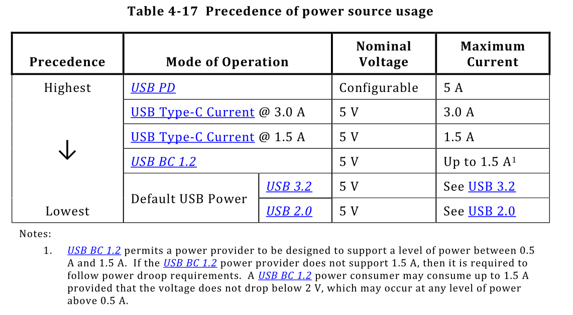
As described by the table, each mode of operation can be superseded by one of the newer ones. USB Type-C Current can provide up to 5V @ 3A.
USB-C Cables/Receptacles
Since we’ll be talking about USB-C, I should briefly cover the cables/plugs and receptacles. USB-C cables are reversible and can have up to 24 pins. Some of these are redundant, but depending on the application, they may not be.
Here are two tables showing the pinout of a Type-C receptacle and a Type-C Plug. Don’t worry too much about what the signals are for yet.
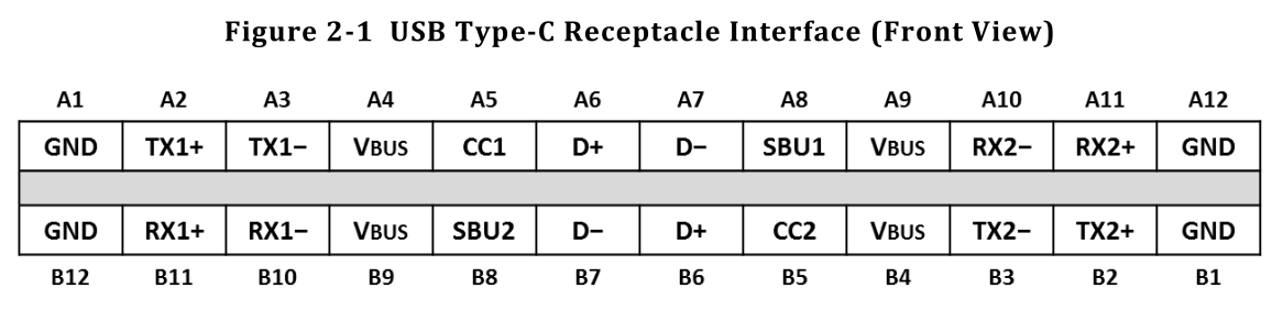
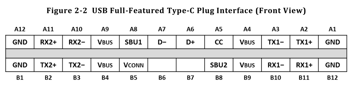
“Legacy” USB-C cables only had Vbus, GND, D-, and D+. Once USB 3.0 came along, it added the high speed signals TX+/TX- and RX+/RX-. Type-C has all of those and then some.
Since Type-C cables can be connected in two ways, the CC lines are used to determine the orientation. All Type-C cables should always have a CC1 line connected and CC2(sometimes labeled as Vconn) NOT connected.
Another very important thing to note is that most Type-C cables DO NOT connect all of the signals! Most inexpensive cables will only have GND, , D+, D-, and CC1. Some will just have GND and VBUS. I think those abominations shouldn’t exist. I even created a USB Cable Tester to root them out and cut them up…
USB Type-C Current
Here’s a quick summary of how USB Type-C Current works. The device providing, or sourcing, power has a pull-up resistor Rp on the CC line and the device receiving, or sinking, power has a pull-down resistor Rd.
Rd is fixed at 5.1kΩ and Rp can change depending on the amount of power available. The figure below from the USB-C specification document shows an example.
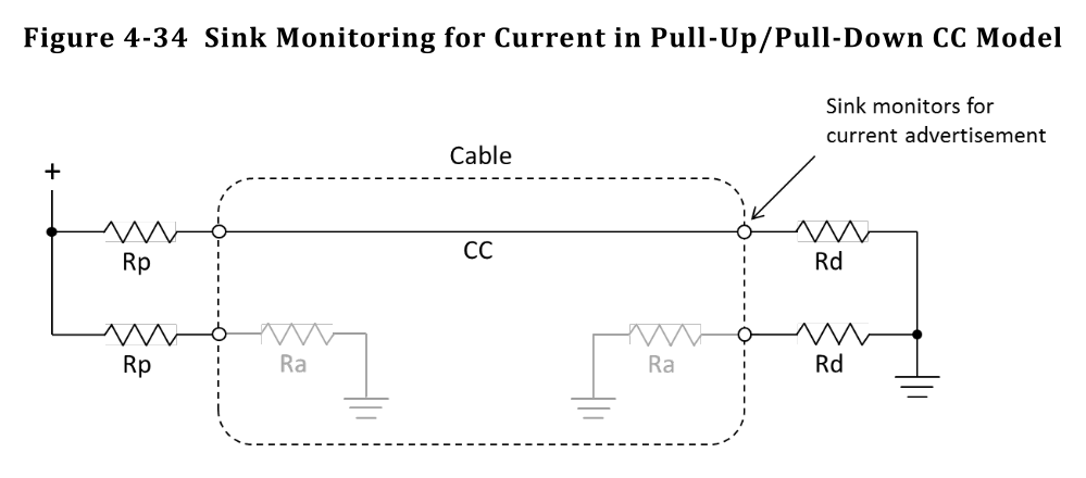
Depending on the source’s pull up resistor (Rp) value, the source can advertise various charge currents. The table below describes the different resistor settings for each advertised source current.
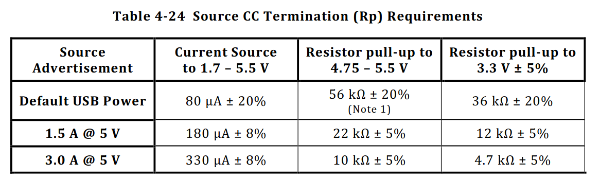
So the CC line lets us know both the orientation of the cable and how much power the source can provide. USB PD can supersede this by communicating over the CC line, but we’re not going to cover that here.
Debug Accessory Mode (DAM)
Time to get to the “fun” bits! The USB-C specification has a section B - Debug Accessory Mode. It explains how to “support” DAM. In short, if both CC1 and CC2 lines are pulled up (as mentioned earlier, only a single one can be pulled up with any cable) a device can enter DAM.
While in DAM, the following signals can be repurposed:
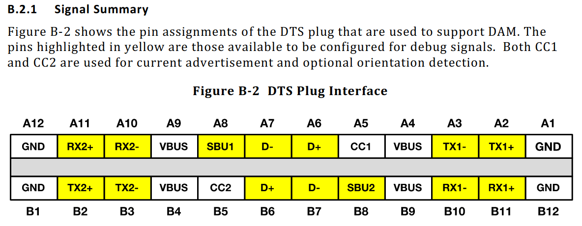
As I mentioned earlier, USB-C cables only pass through CC1 (CC2 is never present. Ok… Technically there’s such a thing as electronically marked cables, see Section 4.9 of the spec, which use it as VCONN, but it doesn’t connect all the way through to both ends of the cable.).
In order to use DAM, we need to have a USB-C plug (or custom cable) to connect both CC1 and CC2.
If the device is in DAM, how can the target tell how much charge current available? There’s another table for that. It uses both CC1 and CC2:
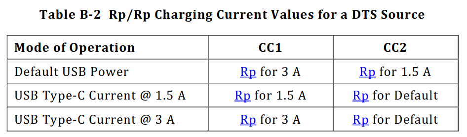
In short, to tell the target that a debugger is connected, both CC1 and CC2 lines need to be pulled up. Once that happens, the highlighted pins in Figure B-2 above can be repurposed for debug signals.
Implementation
Debug Accessory Mode does not specify any standard pinout. It is up to the designer to figure that out. Any of the highlighted pins from Figure B-2 above can be used for any purpose. Here’s what I came up with (Note that this is from the target’s perspective):
- TX1- - SWDCLK
- TX1+ - SWDIO
- TX2- - SWO
- TX2+ - NRST
- SBU1 - VCC(target)
- SBU2 - GND
USB D+/D- stay connected the usual way (and continue to provide USB 2.0 communication with the target). Otherwise we’d need some sort of multiplexer for the USB lines which just adds unnecessary complexity.
NOTE: *I had originally used the RX1/2 lines, forgetting that USB cables crossover tx/rx, which caused issues. I’m using the corrected ones here so no one gets confused
This pinout means that the connector is not reversible. Using the TX and RX lines in a particular way would allow for that, but I decided not to do that (I’ll explain why later.) Technically speaking, a device should not enter DAM unless CC1/CC2 are both pulled up.
In order to do this “properly”, we can use a two comparators(op-amps in my case), an AND gate, and a switch (TMUX1511, in this case). The comparators detect when both CC1/CC2 are pulled up. If both are, the AND gate enables the switches to connect all the signals.
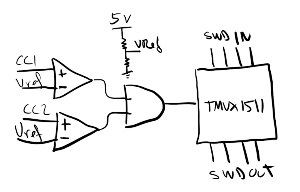
The comparators are needed because the CCx pull-up might be as high as 56kΩ and the targets pull downs are always 5.1kΩ (See tables 4-24 and B-2), which results in a CC voltage of ~0.4V. 0.4V is likely below the AND gate’s threshold, so a simple resistor divider is used to set the comparator threshold level (I set it ~0.2V to be safe.)
Testing
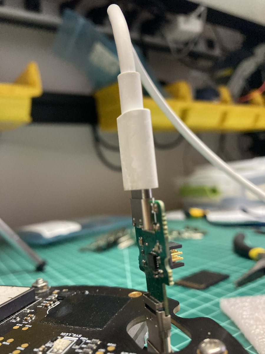
In order to test all this, I first used a USB-C plug breakout board with a few wires 😬. On the other side, I hooked up the circuit mentioned above. (I can’t show the main circuit, unfortunately, since it was from my previous employer). The setup worked though! Time to make some custom boards :D
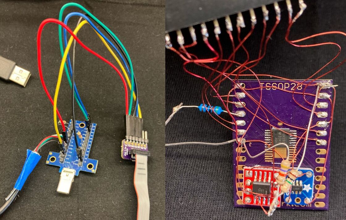
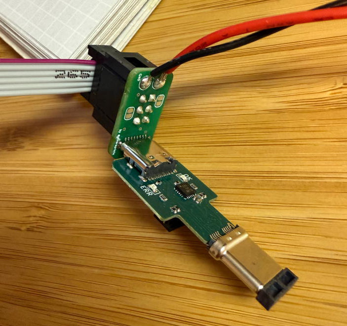
I decided to make a board that passes through power and USB, but hijacks the CC1/CC2 lines to enable DAM. I used an attiny24a to read in the input CCx lines to determine the input charge currents and set the appropriate downstream CC1/CC2 resistors. This would allow for the target device to have accurate information about the source’s capabilities. This was important since we charged large-ish batteries over USB. If a target was connected to a laptop that could only source 500mA, we had to set the battery charge current appropriately.
I used the wrong footprint for the attiny24a 🤦♂️. I ended up hard-wiring the CC resistors for the and it worked :D.
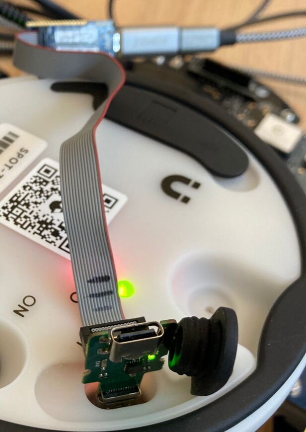
Later on, I updated the design to fix the issues. It used the SBU1/SBU2 signals (VCC/GND on the target) to determine proper orientation. It lit up a green or red LED if the target was plugged in correctly or if it needed to be flipped. It had the standard ARM 10-pin connector to use a regular debugger..
The only problem was… I had to program the attiny24 somehowi!
So I made another programmer over USB-C 😂 This one used SPI instead of SWD. I also got the MISO/MOSI lines flipped, so had to use some jumper wires to program.
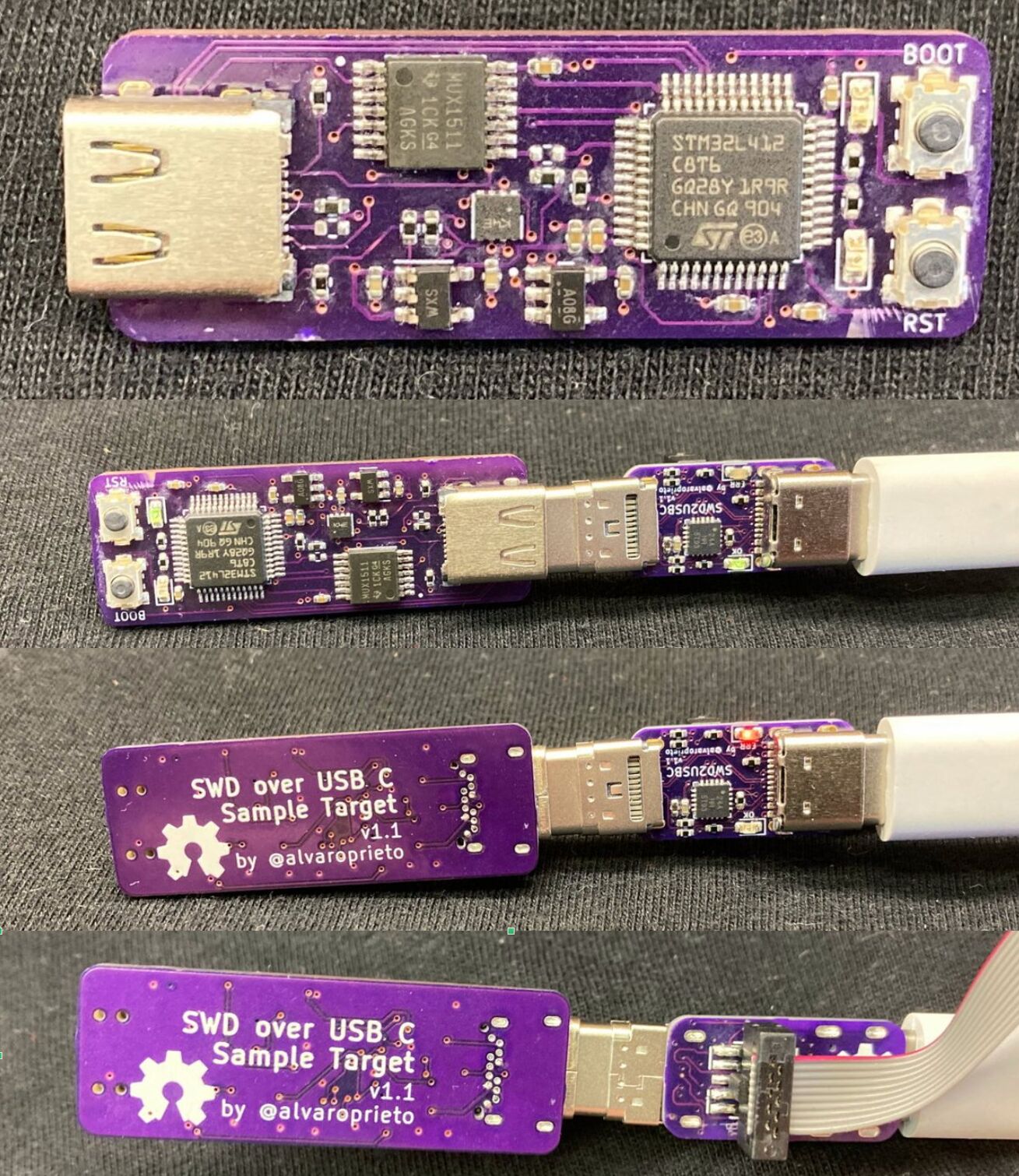
I decided to make a test target with all the features mentioned above. It’s just an STM32L4 with USB and a couple of LEDs (along with all the CCx detection fun). You can see how the LED is red when it’s plugged in backwards. After much pain soldering on those USB-C connectors, it all worked!
New Designs
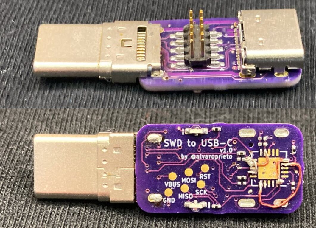
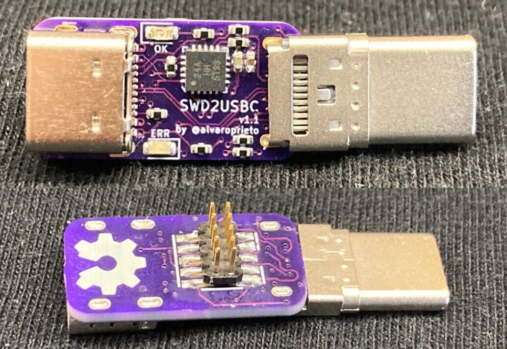
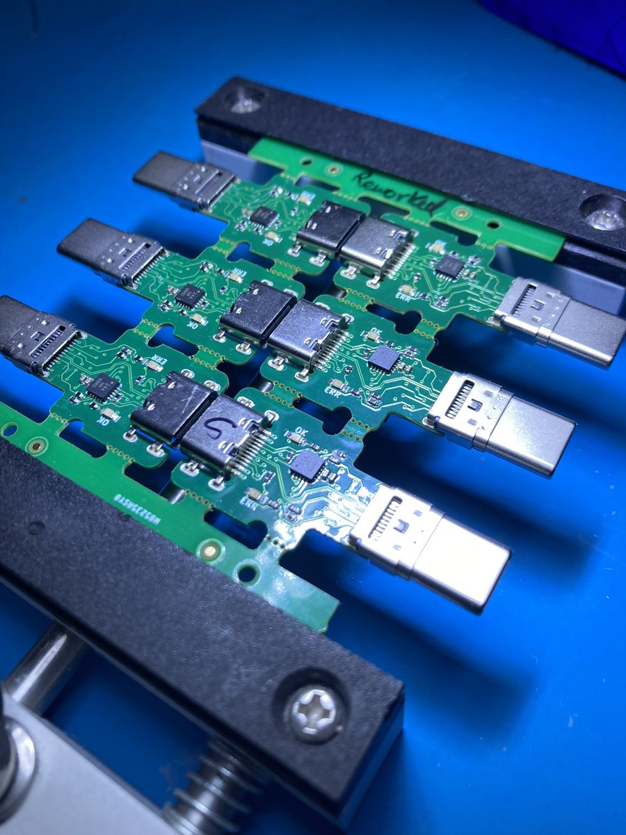
I re-designed the board to be more easily produced and hopefully allow for a case at some point. This was also the first time I used PCBWay for assembly, which was a neat.
They did the panelization, and it came out fairly well. I screwed up my BOM so I had to swap a couple of resistors around, but otherwise they worked great!
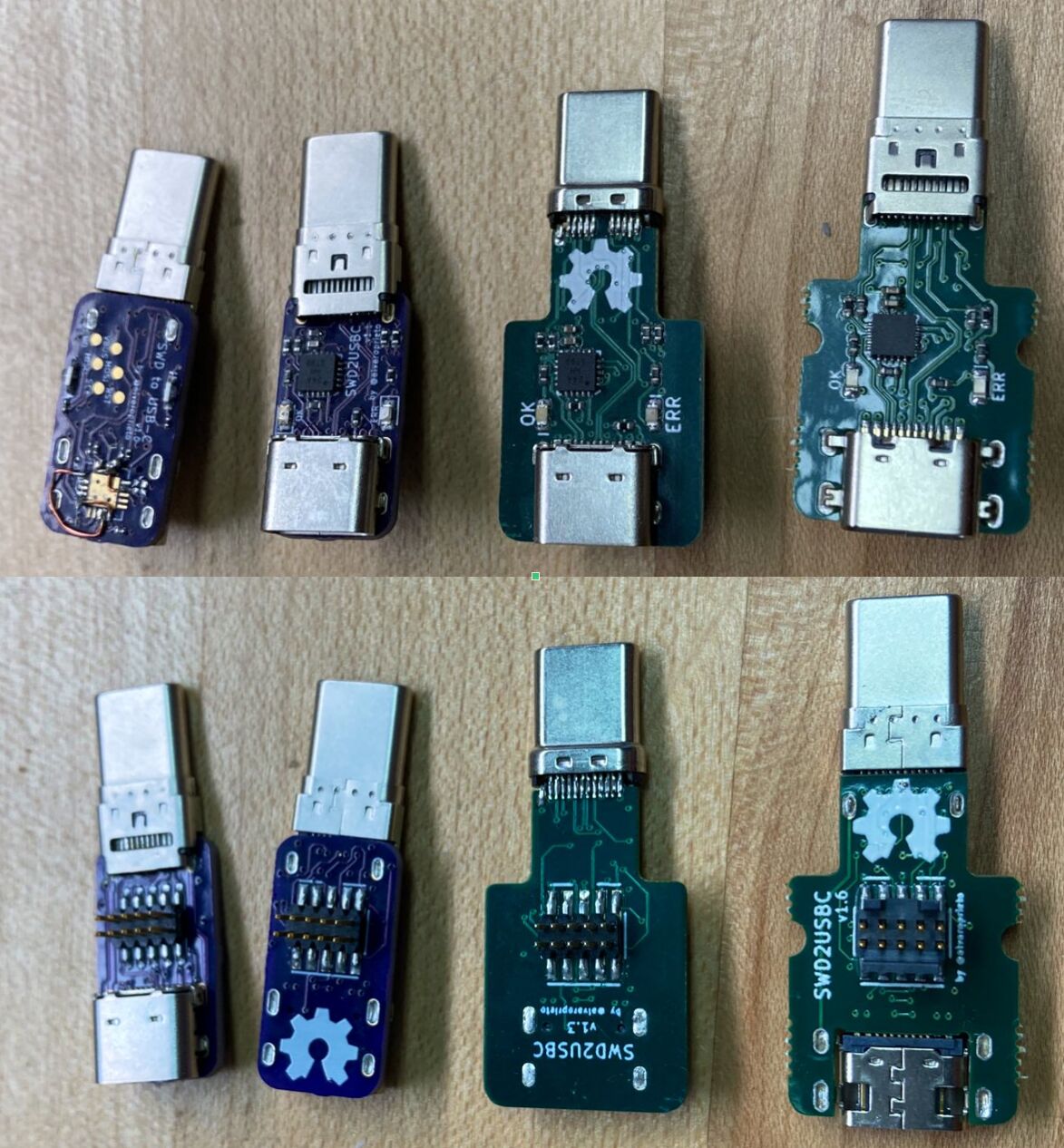
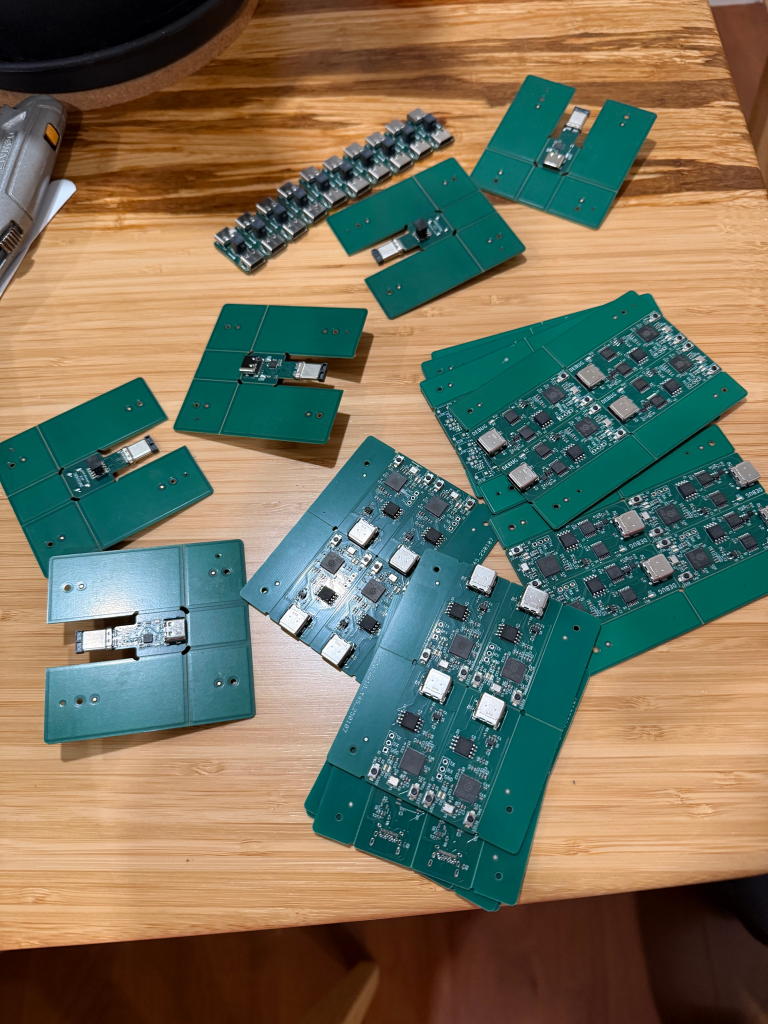
Here’s a photo of a few generations. The first three were hand assembled by me 😬. USB-C plugs are no fun to solder.
Possible Improvements
So what’s next? First, I made 20 of these. We used them at work successfully for months! That being said, I was already thinking of ways to improve the design.
Due to the form factor, quite a bit of stress is placed on that plug from the USB cable pulling on it. We had several USB-C plugs break off due to cables puling the wrong way.
Ideally, I’d like to switch to the form factor below, where the main PCB and USB receptacle are on one side, and a USB cable with the plug is attached to it. This way, it would be much more durable, and I can put things like a CPLD or FPGA to do fun thing on the larger PCB.
Teardown
I had no idea how they make these, so I decided to take a look 😅. Removing one side was fairly easy. Seems like a pretty neat way to attach the USB cable.
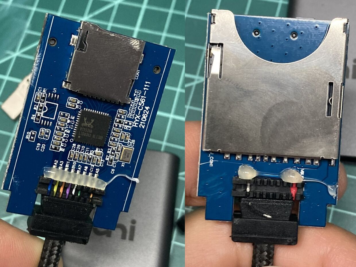
Removing the other end was much more destructive. I had to rip apart the metal case, cut the molded plastic, then remove the second metal shield.
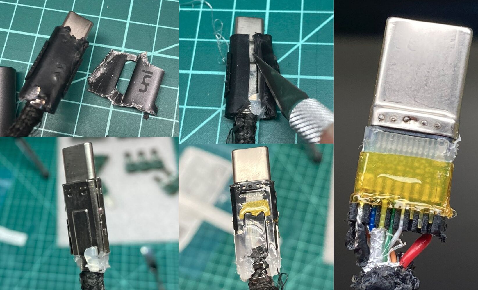
It’s a mini PCB as expected. There were many more layers of tape/plastic/insulation than I expected. They were even nice enough to label the pins!
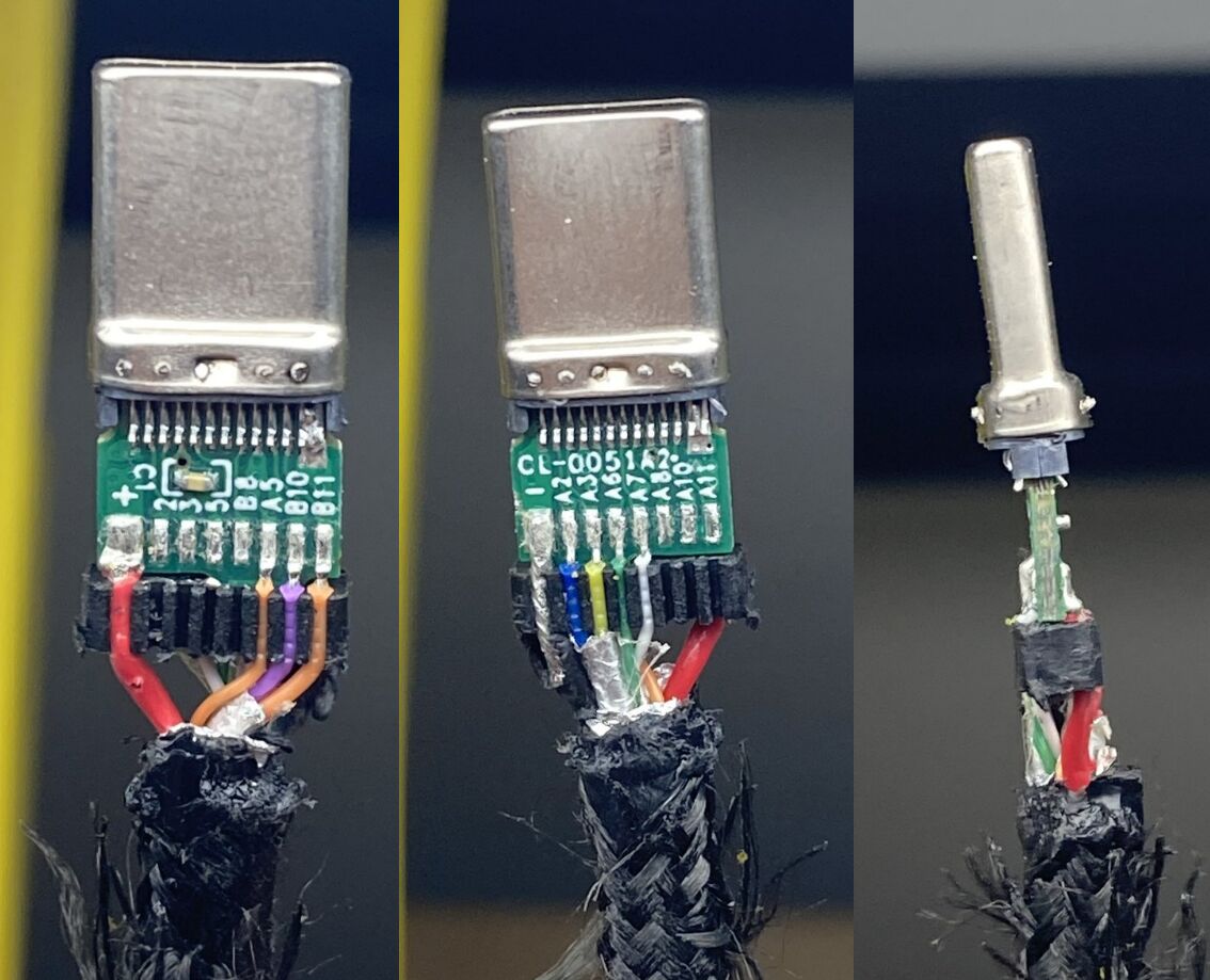
Unfortunately, this project would need a completely custom cable. It would need to connect all of the pins through it, including CC1/CC2, as well as two separate D+/D- pairs. Not cheap, especially for low volumes.
Real World Scenarios
OK, so back to why I didn’t want to make the pinout reversible. Following the USB spec is nice and all, but for hobby projects… 🤷
What if we were to ignore all of the CCx detection stuff and just permanently wire the SWD lines to the USB port? Saves us several components and space! No need for comparators and muxes.
If we had used the RX1/2 lines of the USB-C port, the host would send some test pulses after connecting to try and negotiate USB 3 (or something else). Since we only use the TX lines, there’s a low chance of the host signals causing unintentional trouble over SWD (since they’re receive lines on the host).
If we choose to go this direction, the footprint/component requirements to do this are zero! You’ll still need an adapter board to connect the debugger, but that’s it!
It is also fair to mention that SWD over USB-C does require a full 24 pin USB-C connector, which is more expensive and much harder to solder than the 16, or fewer, pin connectors. Having said that, most contract manufacturers these days can handle them without any problems. Worthington Assembly has a nice article about which are the best Type-C connectors to use.
Low Cost/Complexity Design
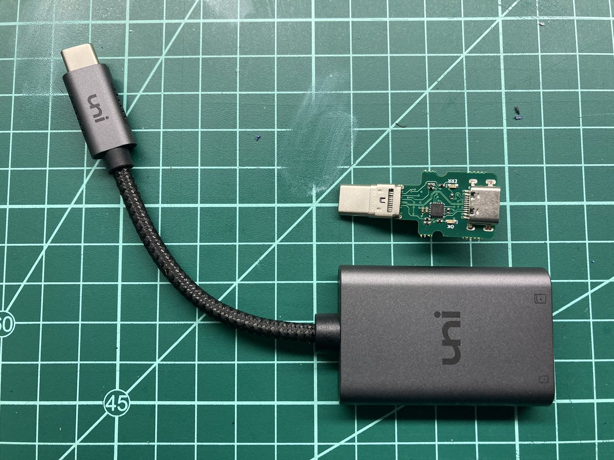
Since manufacturing devices with USB-C plugs and/or custom cables is a pain, I decided to re-design the board entirely. This design has two USB-C connectors and needs a USB 3.0 or Thunderbolt compatible USB-C cable to work.
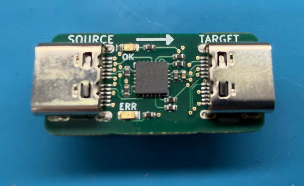
This allows for a more robust (and less expensive) adapter board. Having said that, this breaks DAM compatibility. Since no USB-C cable has both CC1 and CC2 lines, the target cannot use the switch to gate the debug signals. This also means the source current detection must use the non DAM, single CC line, mode.
Since we no longer have to do the source current detection, there’s no need for a small microcontroller on the board anymore. The part count drops significantly. All that is required now is two USB-C connectors, an ARM 10-pin connector, and optionally an LED and resistor connected to the SBU2 line (which is SBU1 on the target, since the cable swaps them).
Below is the schematic for the final version:
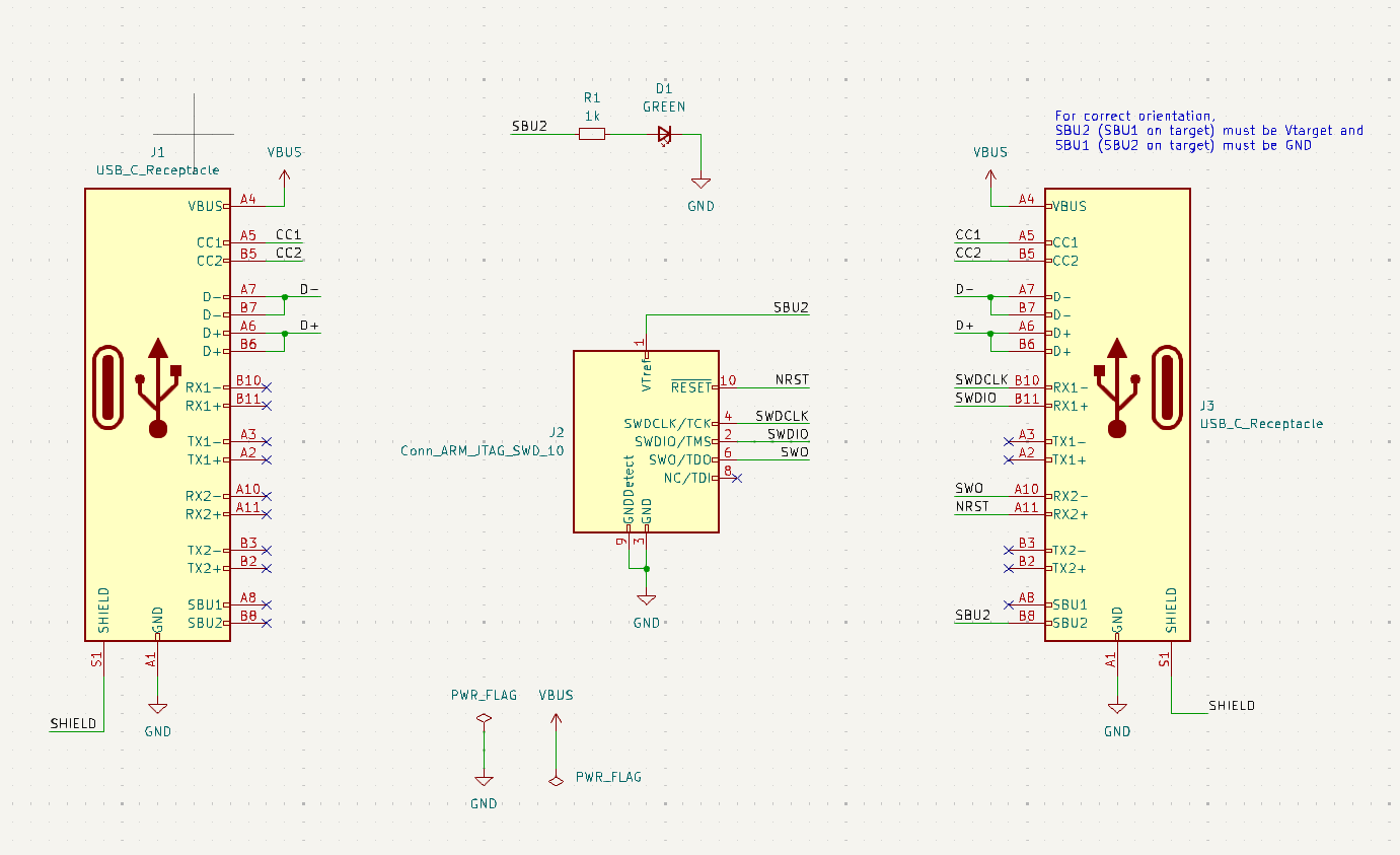
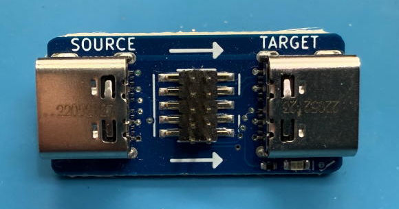
And a photo (this is v4.0). All components are on the same side, further simplifying the design.
Cable Crossover
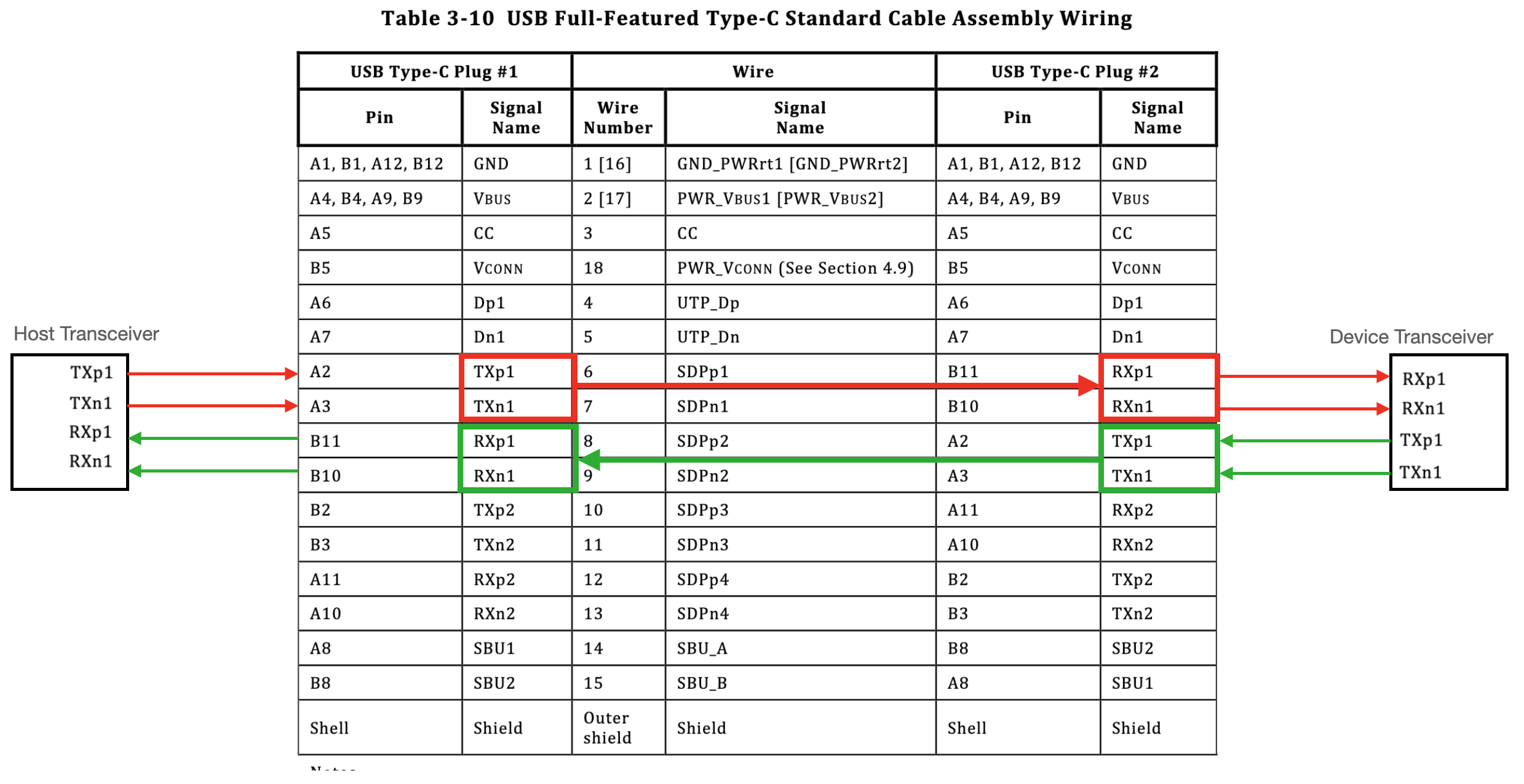
As I mentioned in the implementation section above, I had originally used the wrong pins (RX1/2/+/-). This only worked because we never used USB 3.0/Thunderbolt cables with our devices. Someone spotted the error (Thanks Matthias M.!) and emailed me. Once I plugged in a thunderbolt cable, our devices started getting held on reset, which was not good.
That’s when I re-designed the adapter to use the correct lines and we had to redesign our target board as well to use the correct pins. Whoops!
Here’s the table Matthias sent explaining the crossovers nicely (Note that SBU1/SBU2 also get swapped):
Examples!
Does this sound like something useful? Wouldn’t it be nice to have working examples? Well you’re in luck!
Since I don’t want to have to do this again, I decided to re-design and re-test all of the boards and release them as open source hardware for everyone to use. (They already were, but the documentation was… lacking.)
All of the files for this project can be found in the swd2usbc Github Repo. All PCB’s can be easily ordered from JLCPCB. I added LCSC part numbers for everything in KiCad.
The examples consist of the following:
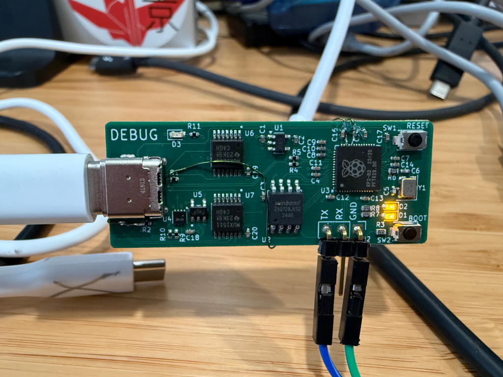
SWD2USBC
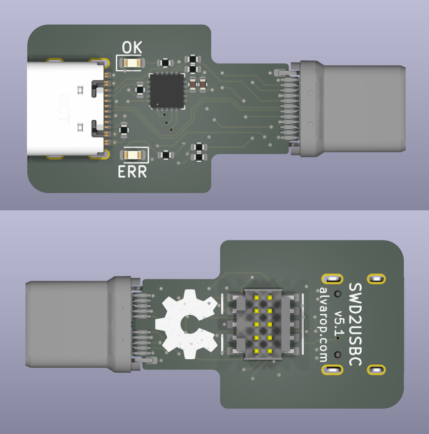
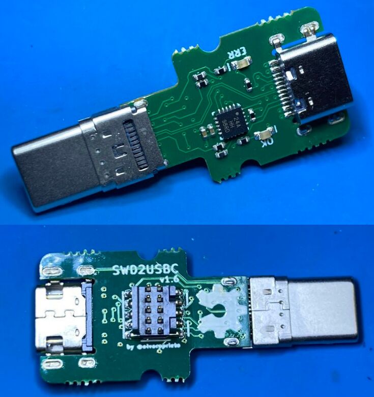
Full featured adapter with Debug Accessory Mode support. Includes an ATTiny microcontroller to set the correct pull-up resistors on CC1/CC2 to provide accurate charge current to the target. Has a USB-C plug so no extra USB-C cable required. Use this to debug the Sample Target.
SWD2USBC Firmware
The ATTiny firmware doesn’t do much. It reads the voltage on the CC1/CC2 line that is pulled up and determines the available charge current. It then pulls up CC1 and CC2 to provide the charge current to the device under Debug Accessory Mode.
SWD2USBC Basic
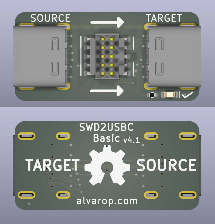
Simple adapter with no Debug Accessory Mode. Assumes target SWD lines wired up directly to TX1/2 as listed above. Requires USB3/Thunderbolt C to C cable to connect to target. Use this with the Sample Target Basic.
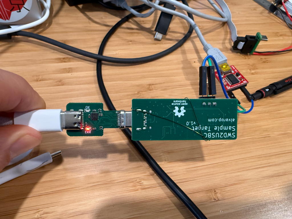
Sample Target
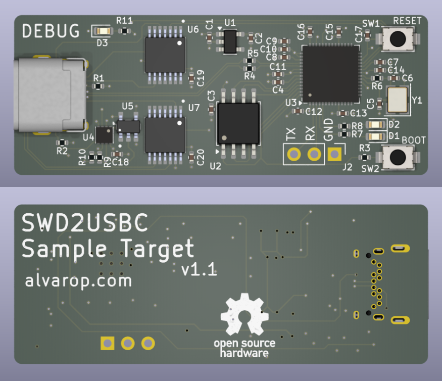
Example target device. Fully featured with CC1/CC2 comparators to connect/disconnect SWD lines if Debug Accessory Mode is active. Target is an RP2040 instead of STM32 since it’s easier to source. Use SWD2USBC to debug this board.
Sample Target Firmware
The sample target firmware does basic USB charge detection using the CC lines. When the Debug Accessory Mode is enabled, both CC1/CC2 are used, otherwise, the single CC line is used. There’s an LED (D3) which lights up when Debug Accessory Mode is enabled.
The charge current is printed out over UART, but it is also displayed using the two LEDs. The blink patterns are:
- 500mA - LED1 (D1) blinks
- 1500mA - LED2 (D2) blinks
- 3000mA - Both LED1 (D1) and LED2 (D2) blink at the same time
- Other/Error - Both LED1 (D1) and LED2 (D2) alternating blink
Sample Target Basic
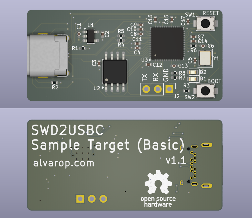
Basic example target. Similar to the sample target above, but does not include any comparators/switches. SWD lines are directly connected to the USB-C connector. Use this with the SWD2USBC Basic.
SWD2USBC Programmer
Simple adapter PCB to connect the AVRISP V2 connector to USB-C to program the ATTiny in the SWD2USBC device.
Putting it All Together
Here are some examples:
Sample Target Connected to 3A capable port
The extra wires you see are the CC-lines going to the RP2040’s ADC’s. I forgot to include them in this revision but have fixed it in the updated files.
SWD2USBC In Action
Properly oriented connection.
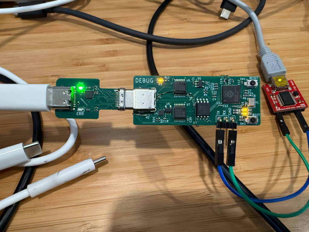
Reversed connection (red/error LED lit up on SWD2USBC)
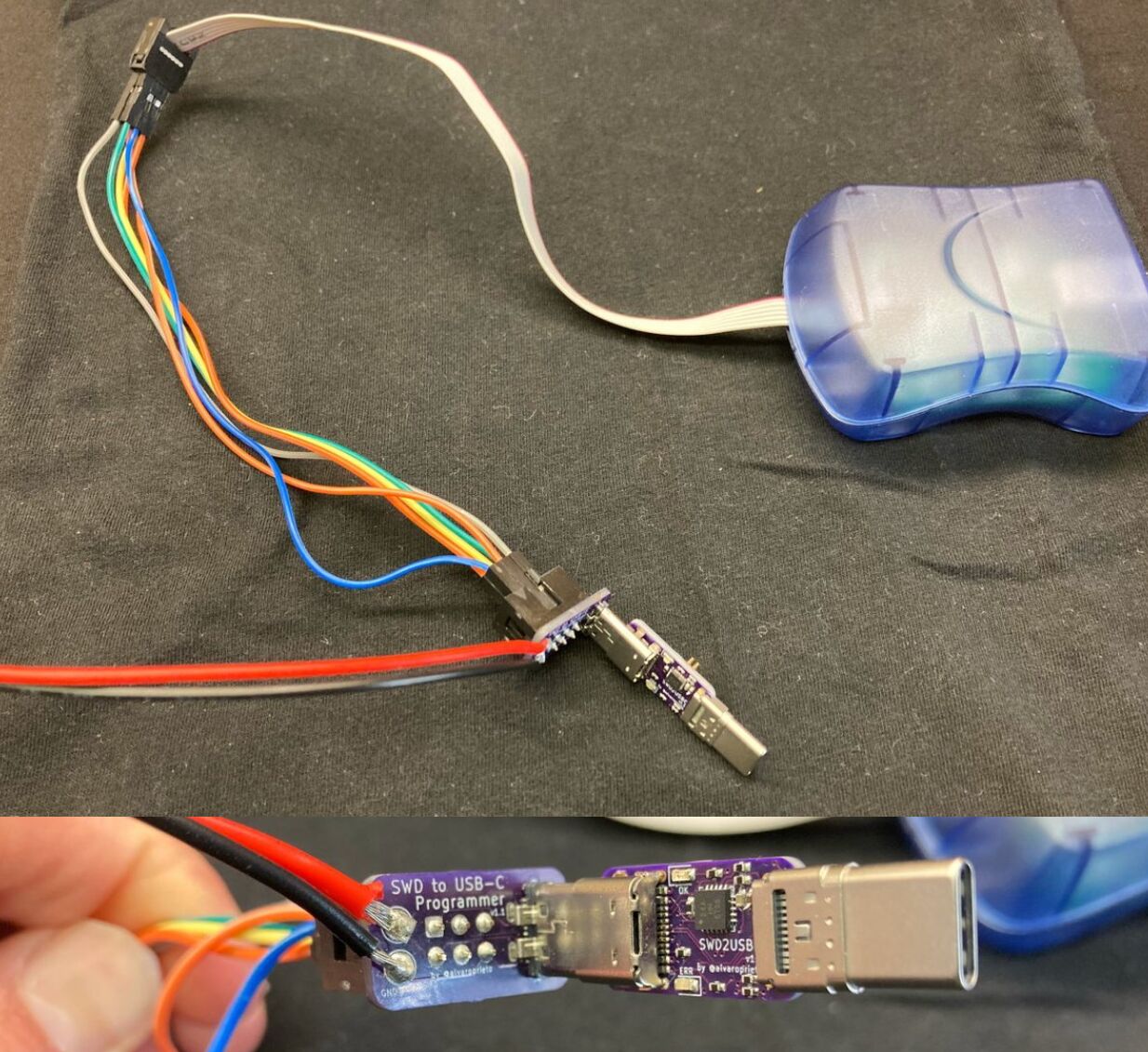
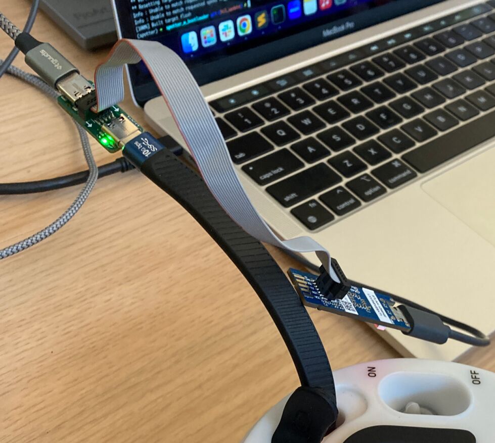
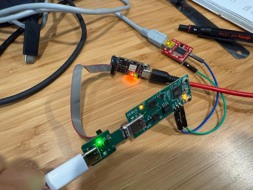
Debugger Attached
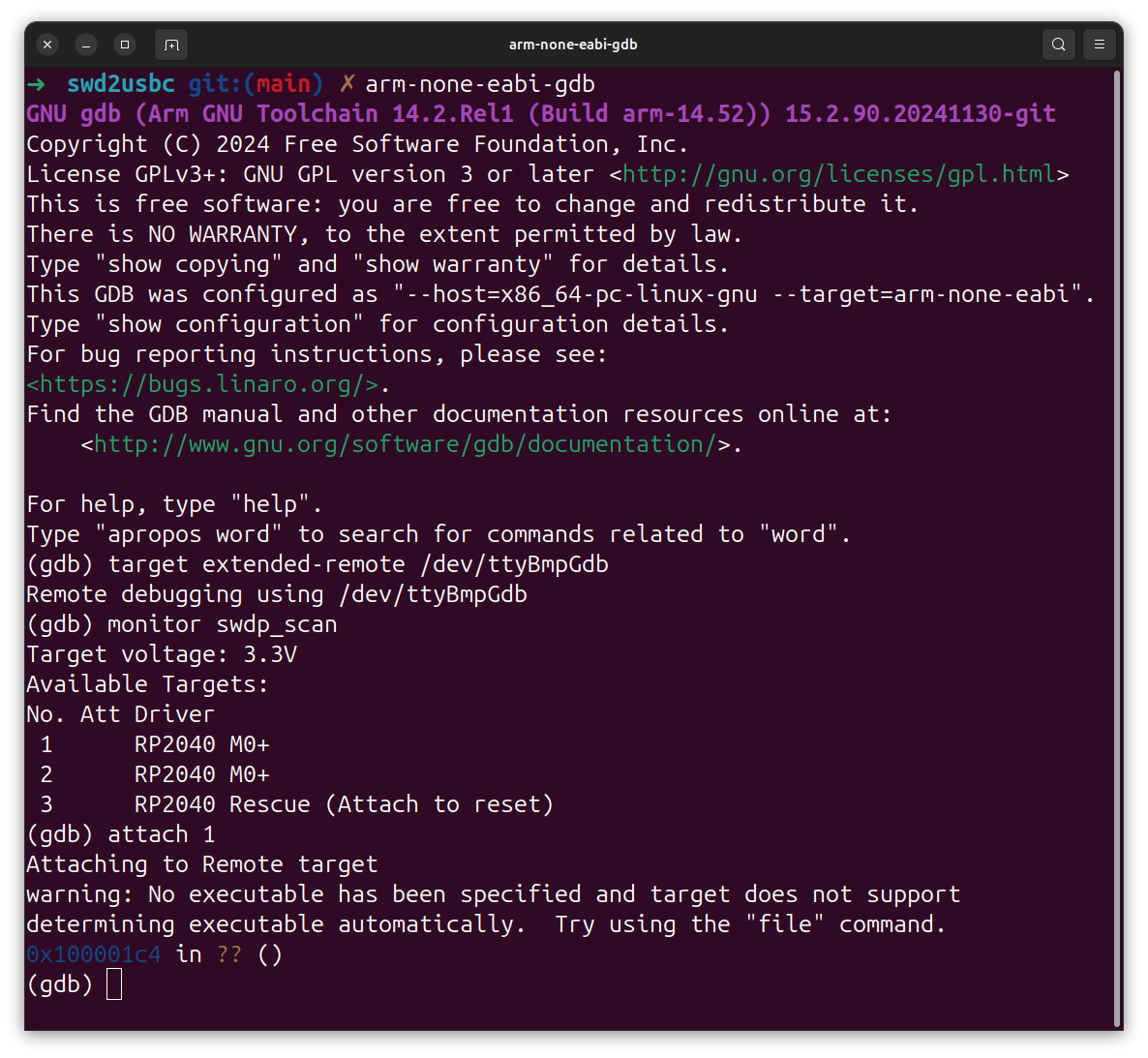
Here’s a complete setup using a Black Magic Probe to attach to the RP2040 through USBC
And the GDB session:
Conclusions
So which one should you use? Honestly, the “basic” version is probably good enough for most designs. Folks have been using it at the last company I was working at for years and haven’t reported any issues.
If you really must, the DAM-compatible version works great! The adapters are much more expensive, but they’ll pay for themselves in time saved using proper debuggers.
I keep wanting to look into custom cables or making a rigid-flex PCB with a USB-C plug to make it more robust, but I’m not sure it’s worth the effort since the basic one works so well.
Hope this was helpful!